5-Stage Pipelined MIPS processor
Code: github repository
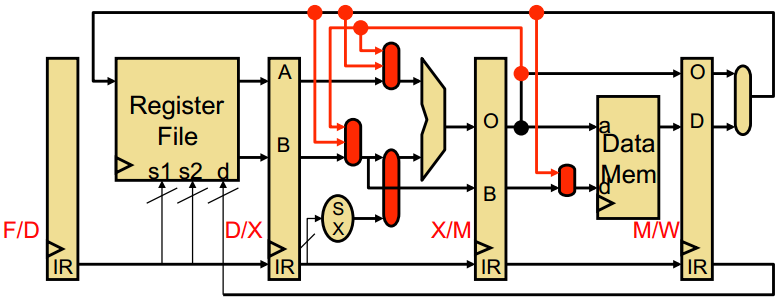
Developed a 5-stage pipelined MIPS processor using the synthesizable subset of Verilog and the Modelsim simulator. The processor executed C programs compiled using GNU GCC. The inputs to the processor were the compiled binary files given in the SREC format which were parsed using an SREC parser and fed into the processor. The architecture of the processor is as shown below:
Developed a 5-stage pipelined MIPS processor using the synthesizable subset of Verilog and the Modelsim simulator. The processor executed C programs compiled using GNU GCC. The inputs to the processor were the compiled binary files given in the SREC format which were parsed using an SREC parser and fed into the processor. The architecture of the processor is as shown below:
| mips_processor_code.zip |
- SREC Parser and Instruction Memory: Byte Addressable memory supporting addressing individual bytes and following ports: clock, address (32-bits), data in (32-bits), data out (32-bits), access_size (2 bits), and read/write (1 bit). Parsed a binary file given in in the SREC format, and stored the contents at the specified addresses in the byte-addressable memory
- Fetch and Decode Stage: Created a fetch module which supplied an address stored in the program counter (PC) register to the address signal of the main memory module. The output from the main memory entered the decode module through an input port of the decode module. Once the address in PC is supplied to the address line of the main memory, the fetch stage increments the PC by 4. Thus, in the next cycle the next instruction will be fetched from the main memory.
- Register File and ALU: Implemented a register file ensuring that the reads happen before writes in the same clock cycle. The outputs of the register file (rsOut, rtOut), the PC and the IR (instruction bits) were passed to the execute stage. Execute stage consisted of a functional unit (integer ALU) which implemented a subset of the operation from the MIPS ISA. The branches were resolved in the execute stage and the effective address was also computed in the execute stage.
- Data Memory and WriteBack: Implemented the Data Memory and initilised it using the SREC files. Also implemented the writeBack logic to update the register file in each cycle.
- Stalling and Bypassing/Forwarding: Pipelined the processor such that the instruction execution was overlapped across all the stages mentioned above. Implemented the basic method to avoid RAW hazards. Also implemented M/X, W/X, W/M forwarding.
1-bit Mirror Adder: Schematic --> Layout --> Extraction
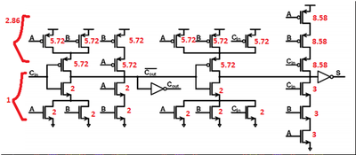
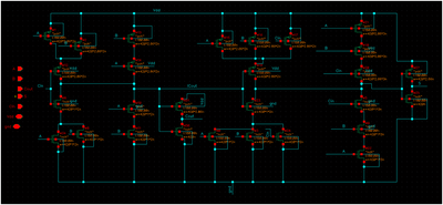
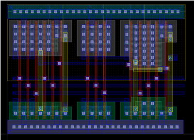
Designed and layed-out a single bit full adder.
Performed analysis pertaining to the transistor sizing, critical path, power consumption and propagation delay.
Compared the post-layout results with schematic simulations.
Specs:
Performed analysis pertaining to the transistor sizing, critical path, power consumption and propagation delay.
Compared the post-layout results with schematic simulations.
Specs:
- Worst case propagation delay < 375ps
- Average Power Consumption < 200uW
- Rise/Fall time of inputs = 50ps
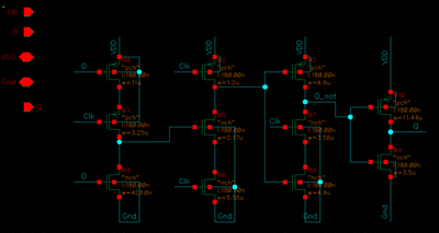
High Performance D-Flip Flop - Dynamic TSPC (True Single Phase Clock)
Part1 - Flip Flop Design
Designed a high performance D-Flip-Flop (DFF). Performed a literature review of various flip-flop topologies and chose the Dynamic TSPC topology for implementation based on the comparitive analysis.
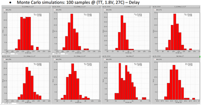
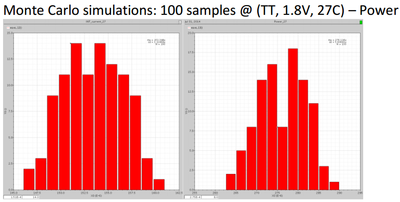
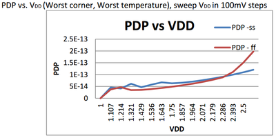
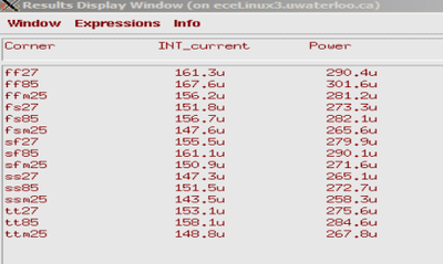
Performed analysis using the following metrics:
• Data-to-output (tp D-Q), Setup time (tp Setup), Clock-to-output (tp C-Q), Average Power (Pavg)
• Considered the following Corners: SS, SF, TT, FS, FF and Temperatures: -25C, 27C, 85C
• PDP vs. VDD (Worst corner, Worst temperature), sweep VDD in 100mV steps
• Monte Carlo simulations: 100 samples @ (TT, 1.8V, 27C)
Results:
Part2 - Pipelining
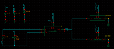
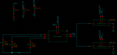
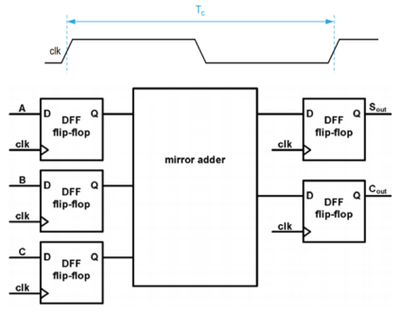
Used the DFF designed in Part1 and the 1-bit mirror adder designed above to implement a pipelined sequential system.
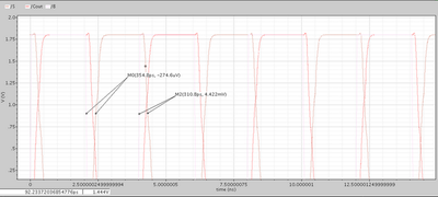
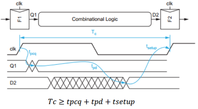
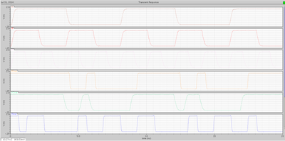
Determined the maximum possible frequency at which the clock can be operated such that the system still operates correctly at (Worst corner, 1.8V, Worst temperature).
Maximum Frequency Obtained = 1.6GHz
